Project Overview
Goal
The goal of this project is to design and fabricate an open-source Bluetooth Low Energy (BLE) ASIC system on chip (SOC) using the SkyWater SKY130 130nm open-source semiconductor process. The completed chip will serve as a fully documented, silicon-proven BLE controller that students, hobbyists, and organizations such as ChipForge at Iowa State University can study, modify, and build upon, filling a gap where no open-source and fabricatible BLE ASIC currently exists.
Background: Bluetooth Low Energy (BLE)
Bluetooth Low Energy (BLE) is a low-power wireless communication protocol operating in the 2.4 GHz frequency band. It is ubiquitous in consumer electronics (fitness trackers, medical sensors, IoT devices), yet every commercial BLE chip is closed-source, preventing users from inspecting, modifying, or learning from the underlying hardware. A complete BLE controller is organized into three layers:
- Host Controller Interface (HCI): The boundary between the host processor and the BLE controller. Commands and events are exchanged here using a standardized packet format defined by the BLE specification.
- Link Layer (LL): The core of the digital design. Manages the BLE state machine, packet framing, frequency-channel hopping (CSJackson algorithm), CRC generation, data whitening, serialization, and connection procedures.
- Physical Layer (PHY): The analog RF subsystem. Modulates and demodulates the 2.4 GHz GFSK signal using a PLL, low-noise amplifier (LNA), power amplifier (PA), RF switch, mixers, and ADC/DAC.
This project targets BLE 4.0 compliance, implementing the minimum mandatory feature set: transmitting and receiving packets, Connection State support, and scannable advertisements.
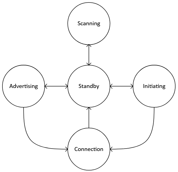
Figure: BLE Link Layer State Machine — the states implemented in our digital design
Background: Digital ASIC Design on the SkyWater SKY130 Process
An Application-Specific Integrated Circuit (ASIC) is a chip designed for a particular function, as opposed to a general-purpose processor. The SkyWater SKY130 is a 130nm open-source Process Design Kit (PDK) developed jointly by SkyWater Technology and Google, making silicon fabrication accessible to academic teams and independent designers for a fraction of the cost of commercial chip fabrication.
This project targets tapeout via the ChipFoundry Tiny Tapeout shuttle process, using the Caravel management core frame to accommodate the analog I/O required by the RF subsystem. The digital design follows an industry-standard RTL-to-GDSII flow: HDL description in Verilog → synthesis → place-and-route → post-layout parasitic extraction → tapeout submission. All tooling (OpenLane, Magic, Xschem, KLayout, BabbleSim, Bumble) is open source.
Top-Level System Design
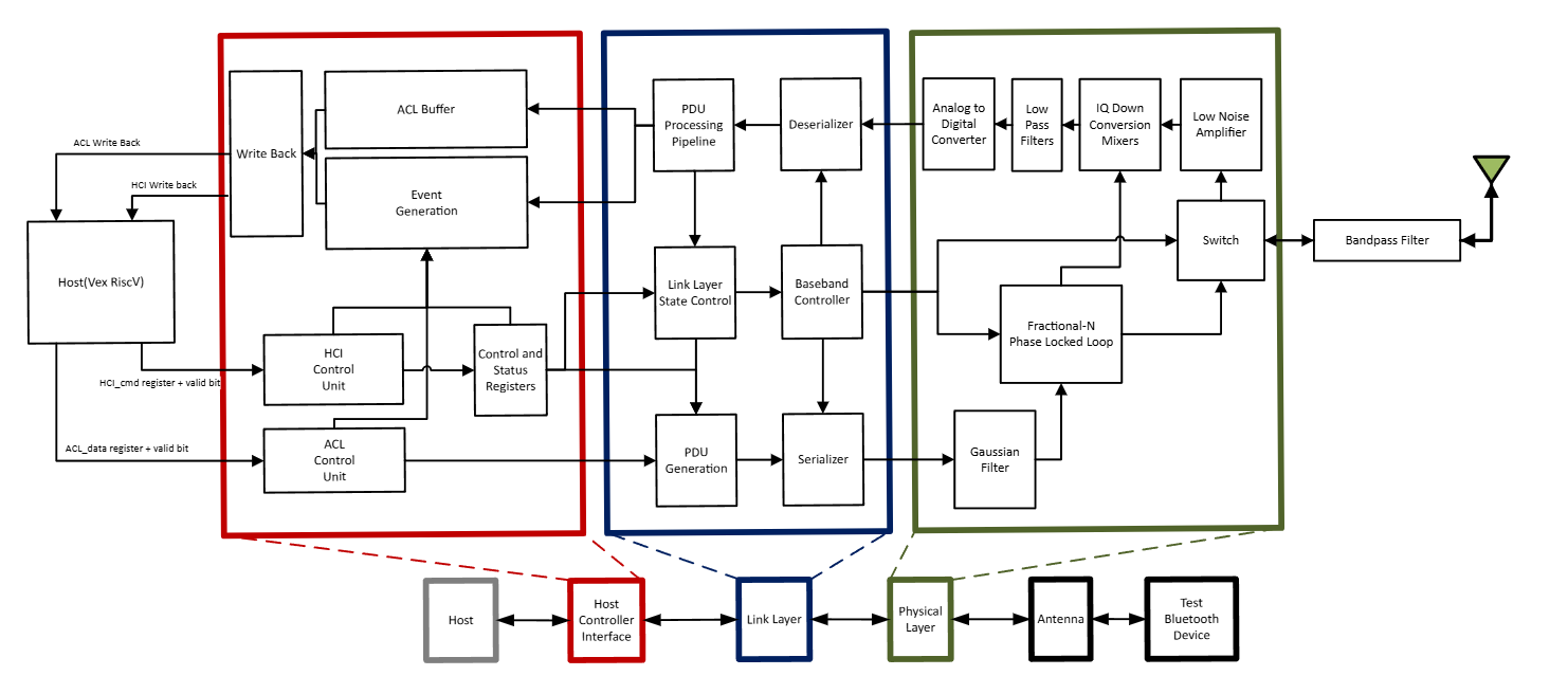
Figure: Top-Level Design — full SOC architecture showing HCI, Link Layer, and PHY subsystems
Team Structure
The team of eight is split into two parallel sub-teams that converge at integration:
-
Digital Team: Parker Pederson, Zane Salti, Tyler Bibus, Aiden Han-Lindemyer, Akash Gojuru.
Responsible for HCI and Link Layer RTL design, software simulation environment (Bumble + BabbleSim), FPGA-based RTL verification, Sky130 synthesis and tapeout flow. -
Analog Team: Jackson Doyle, Seth Klaassen, Daniel Pytel.
Responsible for the Physical Layer: fractional-N PLL/VCO, low-noise amplifier, power amplifier, RF switch, mixer, and ADC. Tools include MATLAB, Cadence, Xschem, and MAGIC.
Timeline & Progress
The project follows a hybrid agile model broken into three phases, spanning two semesters:
- Phase 1 - Foundation & Scoping (Complete): BLE specification analysis, toolflow onboarding, and system scope definition. Early toolchain challenges (SSH, statfs, VM configuration) were resolved and accounted for in the adjusted schedule.
- Phase 2 - Architecture & Simulation: Building a simulation-first workflow using Bumble (Python BLE host) and BabbleSim (wireless modem simulator) as a golden model for validating digital logic before RTL implementation. Parallel analog PHY architecture, PLL topology selection (fractional-N), and component-level design.
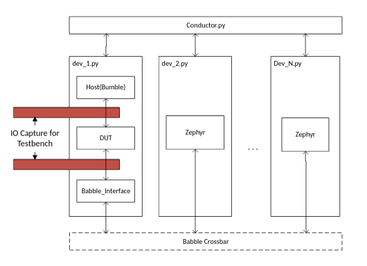
Figure: Digital BLE Simulation Environment — test infrastructure for the Device Under Test (DUT) using Bumble and BabbleSim
- Phase 3 - Implementation & Integration: RTL development, PHY layout, digital-analog system integration, post-layout parasitic extraction, and final tapeout submission to ChipFoundry Tiny Tapeout.
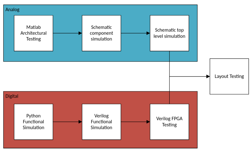
Figure: Testing Plan — end-to-end verification strategy across simulation, FPGA, and silicon phases
Team Members
Zane Salti
Project Lead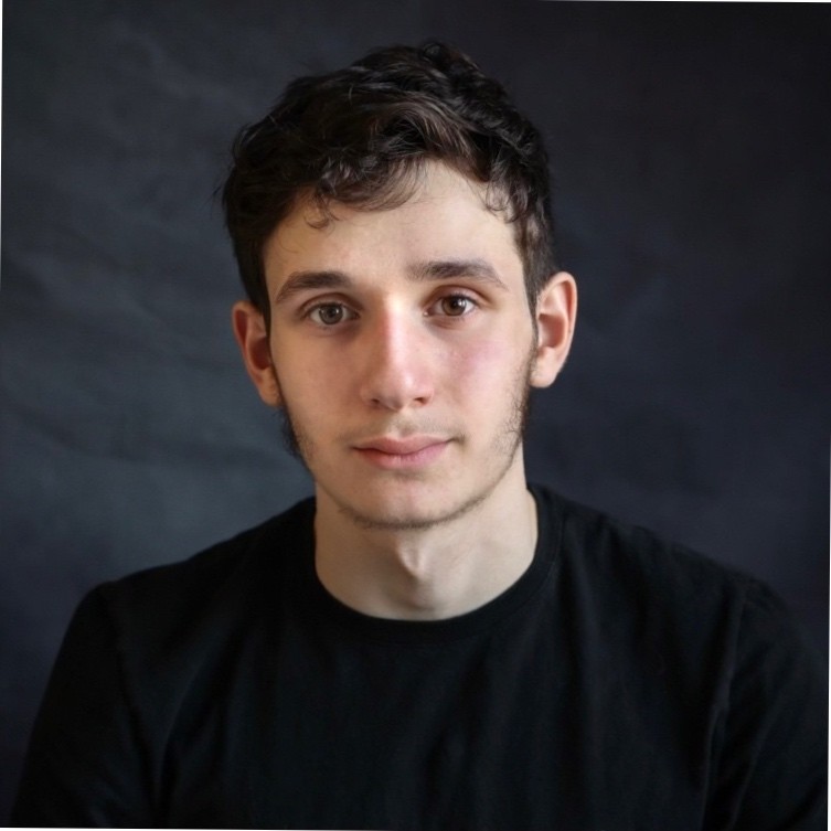
Computer engineering student interested in hardware design, firmware, and RF
Tyler Bibus
Digital Simulation Lead
Computer engineering student with an interest in Digital ASIC design.
Jackson Doyle
Analog Team Lead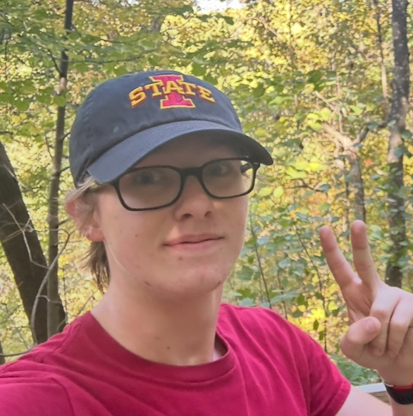
Electrical Engineering student with focus in Power Systems
Akash Gojuru
Digital Design Member
Computer Engineering major focusing on computer architecture and machine learning applications.
Aiden Han-Lindemyer
Digital Testing Lead
Computer Engineering student with interest in firmware and embedded systems architecture
Seth Klaassen
Analog Layout Coordinator
Electrical Engineering major with interest in embedded systems and RF technologies
Parker Pederson
Digital Team Lead
Computer engineering student with a focus on embedded systems architecture, digital design, and VLSI.
Daniel Pytel
Analog Team Coordinator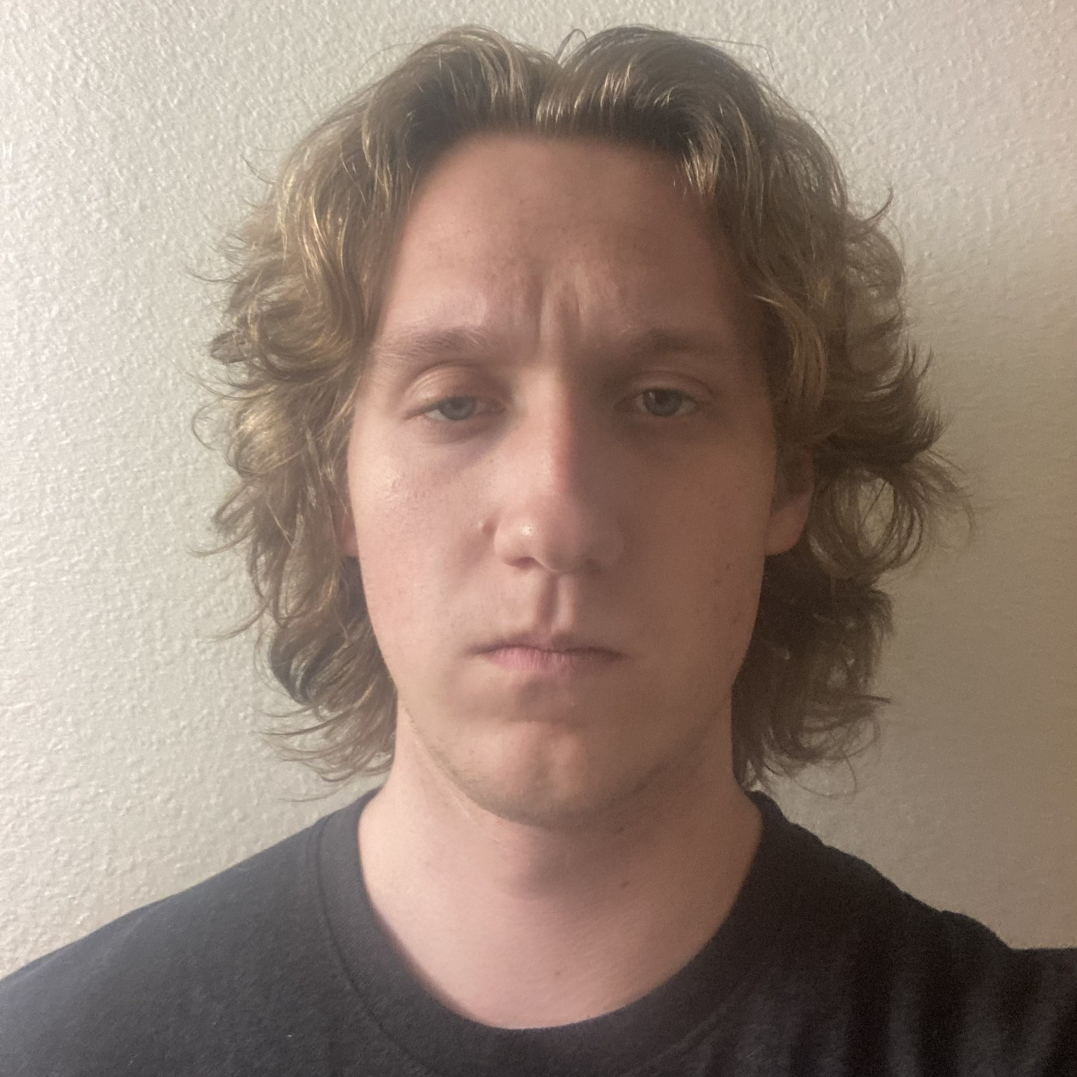
Electrical engineering student, with a focus in VLSI
Weekly Reports
Report 1Report 2
Report 3
Report 4
Report 5
Report 6
Report 7
Report 8
Report 9